A few months ago, I set out to create KiKard, a custom NFC testing board meant for part two of my NFC Card emulation series. It was an ambitious project with some pretty lofty goals, but I felt somewhat confident that I could complete it within a month. Unfortunately, things did not go according to plan, and after three months, I was left with a defective design. Here’s what went wrong.
The Goals

Let’s start with the purpose of KiKard. NFC was the central point for the project, but I also wanted other features to make it a more complete and useful tool.
NFC Emulation
This was non-negotiable and was going to be achieved using an NRF52840. The NRF MCU is capable of NFC tag emulation, and there is already code online that can make it act like a Mifare keycard (which we got stuck on in part one).
NFC Reading
A separate chip was needed to perform the reading, and I chose the ST25R3916. It’s a robust reader, and it also has prewritten code online to perform various attacks on keycards (Flipper Zero).
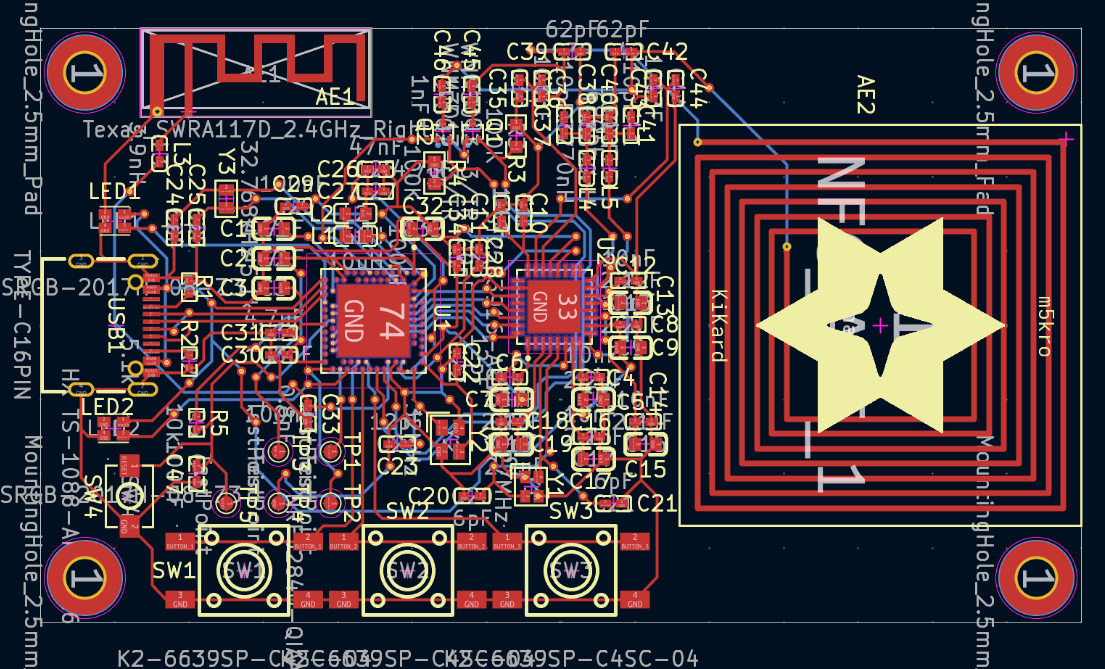
One NFC Antenna
I wanted to have a shared NFC antenna between the NRF and ST25 that would switch between both. This would make the board much smaller and prevent interference from having two antennas right next to each other.
BLE Antenna
This was less of a priority, but the NRF had BLE capabilities, and I wanted to be able to use it in the future for remote control. It could also be used for Zigbee as it shares the 2.4 GHz spectrum.
Schematic

The schematics for KiKard were centered around the two NFC chips. There were plenty of NRF devboard schematics online, and the Nordic documentation also included an example. I used these examples to quickly wire up the NRF MCU, but connecting the ST25 proved more challenging. Thankfully, after some research, I discovered STMicroelectronics’ online tools, which helped calculate some of the component values.
The switching mechanism was another problem. I didn’t fully understand what I was doing, and loosely based my design on the Chameleon Ultra without factoring in the antenna tuning required by the NRF. The NFC would still have theoretically worked, but the range would have been hampered.
PCB Routing

This is where the project failed due to my hubris. After spending a month on the schematic, I got complacent and didn’t conduct enough research for the PCB routing, resulting in numerous rookie mistakes.
Grounding
Let’s start with the grounding. I haphazardly connected all the grounds without thinking, and this could have resulted in a ground loop. Ground loops can interfere with antennas, shortening their range and decreasing overall performance. To solve this, I should have used ground planes to create a return path for all the power.
BLE Antenna
The main issue with the BLE antenna was impedance matching, which is needed to tune the antenna to 2.4 GHz. Most require 50 Ohms to function correctly, as well as carefully placed traces with the right thickness. I didn’t do any of that and just dropped in a premade schematic by Texas Instruments, thinking it would work without extra components.
Signal Traces
The final complication was the signal traces. I had routed many of them through vias, adding parasitic capacitance and inductance. They were also quite long and mismatched, which would have caused even more interference.
Price
After seeing the total, I stopped and thought about the practicality of the project. It would have cost me around $250 to have only two boards made, and the alternatives online were much cheaper. However, I quickly realized why it was so expensive. To manufacture the PCB, I decided to use JLCPCB and their economic PCBA service. When choosing the parts, I selected higher quality C0G/NP0 capacitors to keep the antennas stable. What I didn’t notice was that many of them were “extended” parts. These parts are from third party suppliers, and I had to pay an extra $3 for every single one, resulting in $81 in fees. The worst part, though, was the tariffs. An absurd $60 customs fee was tacked on, and it was incredibly frustrating to see.
During this time, I also decided to check my design with a friend who had more experience than I did. It was devastating to find out that I screwed up almost everything, but I’m glad I didn’t shell out $250 to find out later.
Improvements/Future

I definitely plan on creating a working version of this project. In version 2, simplicity and cost will be the key to success. During my research, I discovered the Seeed Studio Xiao NRF52840, which is only $10 a pop. Not only does it take care of the NRF wiring, but it also comes with a BLE antenna, preflashed bootloader, and battery manager. This will save about $100 from the total and make development much easier. I also want to switch out the ST25 with a cheaper and smaller/simpler reader, such as the PN series from NXP. But NFC reading might be part of version 3, as I still have much to learn about PCB routing.